|
Our group is
interested in low dimensional nano-structured materials (such as 2D TMDC,
graphene, carbon nanotubes, organic molecules) for nanoelectronic and
optoelectronic device applications. The primary focus is in the fabrication of
prototype devices using state of the art nano-scale patterning and lithography
techniques, understanding the fundamental charge transport properties at
different temperature regimes and exploiting those properties for novel
applications. Current research interest includes:
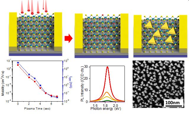
1. Tailoring
the properties of two dimensional (2D) transition metal dichalcogenides (TMDC):
The ability to create and manipulating defects constitutes an essential element
in tailoring the electrical, magnetic, and optical properties of the host
material. Altering the properties of bulk semiconductors by defect engineering
has been successfully used for the development of many novel applications.
Although the role of defects is well understood in bulk semiconductors, it has
received little attention in emerging two-dimensional (2D) layered
semiconductors, preventing their full exploitation for tailored 2D
nanoelectronic and optical devices. Our group is conducting research in
tailoring the properties of 2D TMDC via controlled defect engineering.
Ph.D position available: This is a new research direction and we are
looking for highly motivated graduate students who are keen on contributing many
excellent publications. The students will receive training on state of the art
nano-scale device fabrication techniques including high resolution electron beam
lithography, room temperature and low temperature electronic transport
measurements and opto-electronic properties measurements. Past graduate students
from my group went to industry such as Triquint semiconductors as well as in
prestigious academic institutions such as Purdue University and University of
Minnesota. Many of these students published more than 10 papers each in
high-impact factor paper journals.
Undergraduate research position available: We are also looking for
talented and highly motivated undergraduate student volunteers who are seeking
research challenges and would like to publish papers in high impact factor
journals.
Related publications:
1.
Muhammad R. Islam, Narae Kang, Udai
Bhanu, Hari P. Paudel, Mikhail Erementchouk, Laurene Tetard, Michael N.
Leuenberger, and Saiful I. Khondaker. Electrical
property tuning via defect engineering of single layer MoS2 by oxygen plasma.Nanoscale
6, 10033 (2014).
2.
Udai Bhanu, Muhammad R. Islam,
Laurene Tetard, and Saiful I. Khondaker, Photoluminescence
quenching in gold - MoS2 hybrid nanoflakes. Scientific
Reports 4, 5575 (2014).
3.
Narae Kang, Hari P. Paudel, Michael N.
Leuenberger, Laurene Tetard, and Saiful I. Khondaker, Photoluminescence
quenching in Single-layer MoS2 via Oxygen Plasma Treatment. J.
Phys. Chem. C (2014), DOI: 10.1021/jp506964m.
2.
Graphene: Large scale
assembly and tailoring properties
Graphene, the two dimensional single layer of carbon atoms
arranged in a hexagonal and honeycomb structure, has attracted a great deal of
attention because of its unique electronic properties making them model systems
for the observation of novel quantum phenomenon and building blocks for future
nanoelectronic devices. Graphene can be produced in large quantities and
processed in a form of solution thru chemical exfoliation called graphene oxide
sheets. We have developed multidisciplinary research effort on these materials
with a strong emphasis on both fundamental science and device applications.
Related publications (selected):
-
Daeha Joung and Saiful I. Khondaker, Two
to one dimensional crossover in graphene quantum dot arrays observed in
reduced graphene oxide nanoribbons. Phys.
Rev. B 89, 245411 (2014)
-
Daeha Joung and Saiful I. Khondaker, Structural
evolution of reduced graphene oxide with varying carbon sp2 fractions
investigated via Coulomb blockade transport, J.
Phys. Chem. C. 117, 26776 (2013).
-
Soumen Das, Sanjay Singh, Virendra Singh, Daeha Joung, Janet M. Dowding, Lei
Zhai, Saiful I. Khondaker, William T. Self and Sudipta Seal, Oxygenated
Functional Group Density on Graphene Oxide: Its Effect on Cell Toxicity, Particle and Particle systems Characterization 30, 148
(2013).
-
Daeha Joung and Saiful I. Khondaker, Efros-Shklovskii
variable range hopping in reduced graphene oxide sheets of varying carbon sp2
fraction, Physical Review B, 86, 235423 (2012).
-
Daeha Joung, Virendra Singh, Sanghoon Park, Alfons Schulte, Sudipta Seal, and
Saiful I. Khondaker, Anchoring
ceria nanoparticles on reduced graphene oxide and their electronic transport
properties. J.
Phys. Chem. C, 115, 24494–24500 (2011)
-
Virendra Singh, Daeha Joung, Lei Zhai, Soumen Das, Saiful I. Khondaker, and
Sudipta Seal.
Graphene Based Materials: Past, Present and Future.
Prog Mater Sci vol 56, 1178 (2011).
-
Daeha Joung, Lei Zhai, and Saiful I. Khondaker,
Coulomb blockade and hopping conduction in graphene quantum dots array,
Phys. Rev. B 83, 115323 (2011).
-
Anindarupa Chunder, Tanusri Pal, Saiful I. Khondaker, and Lei Zhai,
Reduced
Graphene Oxide/Copper Phthalocyanine Composite and Its Optoelectrical
Properties,
J. Phys. Chem. C,
2010,
114
(35), 15129–15135
9. Daeha Joung,
A. Chunder, Lei Zhai and Saiful I. Khondaker,
Space
charge limited conduction with exponential trap distribution in reduced graphene
oxide sheets.
Applied Physics Letters 97, 093105 (2010).
10. Surajit Ghosh,
Biddut K. Sarker, Anindarupa Chunder, Lei Zhai, and Saiful I. Khondaker,
Position
dependent photodetector from large area reduced graphene oxide thin films.
Applied Physics Letters
96, 163109 (2010).
11. Daeha Joung,
A. Chunder, Lei Zhai, and Saiful I. Khondaker,
High yield fabrication of chemically reduced graphene oxide field effect
transistors by dielectrophoresis. Nnotechnology 21, 165202 (2010).
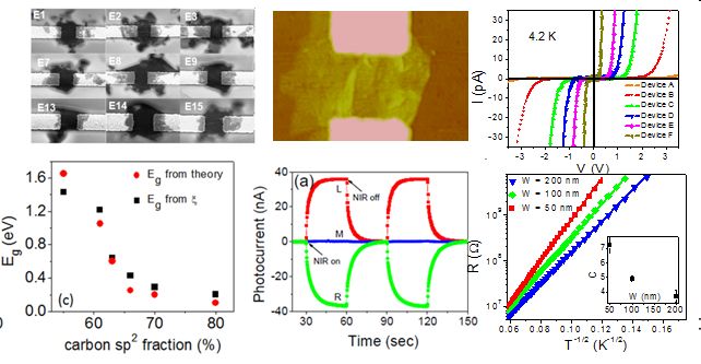
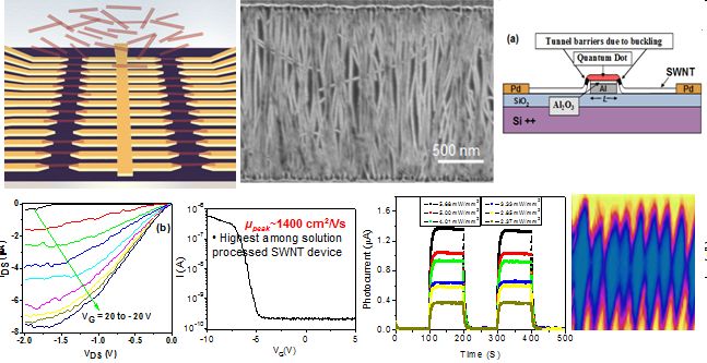
3. Carbon nanotube devices:
Fabrication and device properties
We are using high quality solution processed SWNTs in combination with AC
dielectrophoresis (DEP) to fabricate SWNT field effect transistors (FETs) and
single electron transistors (SETs) with high yield and examining their detailed
electronic transport properties at room temperature as well as at low
temperatures.
Related publications:
-
Biddut K. Sarker, Narae Kang and Saiful I. Khondaker, High
Performance Semiconducting Enriched Carbon Nanotube Thin Film Transistors
Using Metallic Carbon Nanotube Electrode. Nanoscale
6, 4896 (2014).
-
Mohammad R. Islam and Saiful I. Khondaker, Recent
progress in parallel fabrication of individual single walled carbon nanotube
devices using dielectrophoresis (Invited Review). Materials Express
4, 263 (2014)
-
Paul Stokes, Mohammad R. Islam and Saiful I. Khondaker, Low
temperature electron transport spectroscopy of mechanically templated carbon
nanotube single electron transistors, Journal
of Applied Physics vol 114, 084311 (2013).
-
Muhammad R. Islam, Kristy J. Kormondy (*), Eliot
Silbar (*), and Saiful I. Khondaker, A
general approach for high yield fabrication of CMOS compatible all
semiconducting carbon nanotube field effect transistors. Nanotechnology
23, 125201 (2012). ) (*
denotes undergraduate students)
-
Shashank Shekhar, Helge Heinrich, and Saiful I. Khondaker, Huge
Volume Expansion and Structural Transformation of Carbon Nanotube Aligned
Arrays during Electrical Breakdown in Vacuum. CARBON
50 (2012) 1635-1643.
-
Kristy J. Kormondy(*), Paul Stokes, and Saiful I. Khondaker, High
yield assembly and electron transport investigation of semiconducting-rich
local-gated single-walled carbon nanotube field effect transistors,
Nanotechnology 22, 415201
(2011) (* denotes undergraduate
student)
-
Biddut K. Sarker, Shashank Shekhar and Saiful I. Khondaker, Semiconducting
enriched carbon nanotube align arrays of tunable density and their electrical
transport properties. ACS
Nano 5, 6297 (2011).
-
Shashank Shekhar, Mikhail Erementchouk, Michael N. Leuenberger, and Saiful I.
Khondaker, Correlated
breakdown of carbon nanotubes in an ultra-high density aligned array,
Applied Physics Letters, vol 98, 243121 (2011).
-
Shashank Shekhar, Paul Stokes, and Saiful I. Khondaker, Ultra-high
density alignment of carbon nanotubes array by dielectrophoresis,
ACS Nano, vol 5, 1739 (2011).
-
Paul Stokes and Saiful I. Khondaker, Directed
assembly of solution processed single walled carbon nanotubes via
dielectrophoresis: from aligned array to individual nanotube devices,
J. Vac. Sci. Technol. B 28,
C6B7 (2010)
-
Paul Stokes and Saiful I. Khondaker, Evaluating
defects in solution processed carbon nanotube devices via low temperature
transport spectroscopy, ACS Nano Vol 4, 2659 (2010)
-
Paul Stokes and Saiful I. Khondaker, High
quality solution processed carbon nanotube transistors assembled by AC
dielectrophoresis, Applied Physics Letters 96, 083110 (2010)
-
Biddut K. Sarker, M. Arif, and Saiful
I. Khondaker, Near-infrared
photoresponse in single walled carbon nanotube/polymer composite films,
CARBON 48, 1539 (2010).
-
Biddut K. Sarker, M. Arif, Paul Stokes, and Saiful
I. Khondaker, Diffusion
mediated photoconduction in multi-walled carbon nanotube film.
Journal of Applied Physics 106, 074307 (2009).
-
Paul Stokes, Eliot Silbar(*), Yashira M. Zayas(*) and Saiful
I. Khondaker, Solution
processed large area field effect transistors from dielectrophoreticly aligned
arrays of single-walled carbon nanotubes. Appl.
Phys. Lett. 94, 113104 (2009) (*
denotes undergraduate students).
-
Paul Stokes, Liwei Liu, Jianhua Zou, Lei Zhai, Qun Huo and Saiful
I. Khondaker, Photoresponse
in large area multi-walled carbon nanotube/ polymer nanocomposite films.
Appl. Phys. Lett. 94, 042110
(2009)
-
Jianhua Zou, Saiful
I. Khondaker, Lei Zhai and Qun Huo, A
General Strategy to Disperse and Functionalize Carbon Nanotubes Using
Conjugated Block Copolymers, Advance Functional Materials 19, 479 (2009)
-
Paul Stokes and Saiful
I. Khondaker, Controlled
fabrication of single electron transistors from single-walled carbon nanotubes, Appl. Phys. Lett. 92,
262107 (2008).
-
J. Zou, L. Liu, H. Chen, S. I.
Khondaker, R. D. McCullough, Q. Huo, and L. Zhai, Dispersion
of Pristine Carbon Nanotubes Using Conjugated Block Copolymers. Advanced
Materials 20, 2055 (2008).
-
Paul Stokes and Saiful
I. Khondaker, Local-gated
single-walled carbon nanotube field effect transistors assembled by AC
dielectrophoresis, Nanotechnology 19, 175202 (2008).
This article has
been chosen as a feature article and has also been featured in
nanotechweb.org.
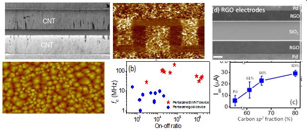
4. High performance organic
electronic devices using CNT and graphene electrodes
A major challenge in improving organic field effect transistor (OFET) device
performance is to reduce the large interfacial barrier between metal and organic
semiconductor (OSC), which results in a low charge injection from the metal
electrode to OSC and limit the performance of OFETs. The large interface barrier
can be originated from discontinuity in morphology, interfacial dipole barrier,
and Schottky barrier. In order to address the challenge of low charge injection,
carbon nanotubes and graphene has been suggested as a promising electrode
material for OFETs due to its high work function and strong π-π interaction with
organic molecules which can reduce the injection barrier at the
electrode/organic interface. We have been working towards that endeavor for the
last several years.
Related publications:
-
Biddut K. Sarker and Saiful I. Khondaker, Lower
Activation Energy in Organic Field Effect Transistors with Carbon Nanotube
Contact. Solid State Electronics 99, 55 (2014).
-
Narae Kang, Biddut K. Sarker, and Saiful I. Khondaker. The
Effect of Carbon Nanotube/Organic Semiconductor Interfacial Area on the
Performance of Organic Transistors, Applied Physics Letters, 101,
233302 (2012).
-
Biddut K. Sarker, and Saiful I. Khondaker, Thermionic
Emission and Tunneling at Carbon Nanotube-Organic Semiconductor Interface. ACS
Nano, vol 6, 4993 (2012)
-
Biddut K. Sarker, and Saiful I. Khondaker, High
Performance Short Channel Organic Transistors using Densely Aligned Carbon
Nanotube Array Electrodes, Appl. Phys. Lett. 100, 023301 (2012)
-
Biddut K. Sarker, Jianhua Liu, Lei Zhai, and Saiful I. Khondaker, Fabrication
of Organic Field Effect Transistor by Directly Grown Poly(3 Hexylthiophene)
Crystalline Nanowires on Carbon Nanotube Aligned Array Electrode, ACS
Appl. Mater. Interfaces 2011, 3, 1180–1185.
-
Biddut K. Sarker, Muhammad R. Islam, Feras Alzubi,
and Saiful I. Khondaker, Fabrication
of Aligned Carbon Nanotube Array Electrodes for Organic Electronics Devices,
Mater. Express 1, 80-85 (2011)
|