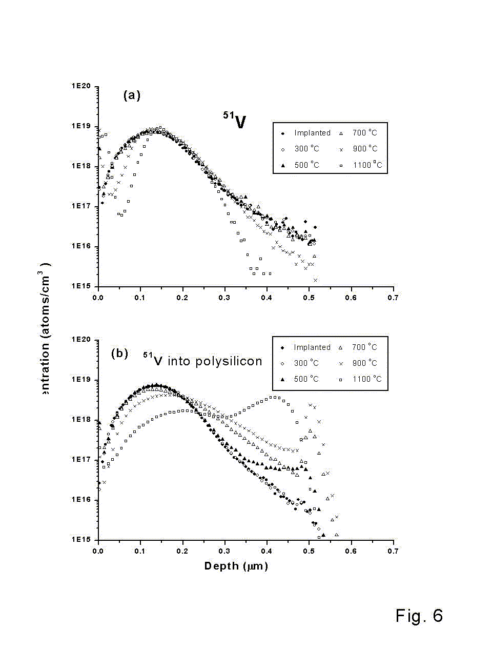
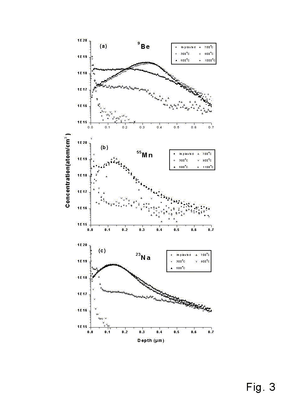
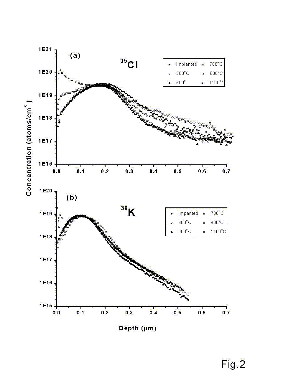
Ion Implantation was carried out by outside vendors. The typical does is 1E14 to 1E15 atoms/cm2. The implant energy ranging from 50 to 1800 keV. All the ion-implanted samples were annealed under flowing Ar at temperature 300, 500, 700, 900, and 1000 C in quartz tube. After annealing, a CAMECA IMS-3f is used for the SIMS analysis of impurity profile. Eighteen elements have been studied so far. The results will be presented at the AVS meeting this fall. Some examples are shown here. Vanadium diffusion in crystalline Si and poly-Si. Be, Mn, & Na diffusion in Si. Cl and K diffusion in Si.
In conjunction with the experimental work, we are also in the process of developing theoretic models of impurity-defect interaction to explain the experimental findings. We will start with TRIM calculations of dopants and defects profiles and use them as input for the PDE solver.
Another related area of research is the development of diffusion barrier for Cu. Transition metals are detrimental to the silicon-based devices. However, with the shrinking of the semiconductor devices, Cu interconnects become unavoidable. We noted that CVD nanodiamond thin film could be used as diffusion barrier for Cu. Preliminary resuts showed that Cu implanted into nanodiamond do not move at 500 C