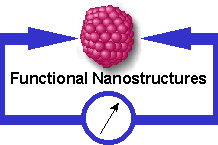

| GOAL | To create a model program of cooperative action between the university and high-technology industry that will enhance the UCF-Physics department. |
| STRATEGY | Use a focussed series of faculty hires in the area of functional nanostructures to build a world-class effort in this field. |
|
|
|
|
|
|
|
|
|
|
|
|
|
|
|
|
|
|
|
|
|
|
|
|
|
|
|
|
|
|
|
|
|
|
|
|
|
|
|
|
|
|
|
|
|
|
|
|
|
|
|
|
|
|
|
|
|
|
|
|
|
|
|
|
|
|
|
|
|
|
|
|
|
|
|
|
|
The microelectronics industry has maintained this furious pace for a quarter of a century, and there are well-established "roadmaps" indicating where the near-term development must take place. An example of the impact of Moore's Law on some of the basic microelectronic parameters is shown in Table 1 [2]. The most often quoted number is the size of a CMOS transistor gate (L_gate), which scales downward in size as the minimum feature size is reduced. The current state of the art is "quarter micron" technology for production, with 0.18 micron (or 180 nm) being the next benchmark on the roadmap. Other component sizes also must scale downwards to maintain the pace of growth implied by Moore's law. By the year 2004, the oxide gate thickness will need to reach a level of only 1.6 nm, not much larger than the thickness of the "native oxide" that spontaneously forms on the surface of a silicon wafer!
Despite this phenomenal past progress, and current optimism about the ability of extensions of current technology to remain on the "roadmap", there are some fundamental problems just ahead. There is nearly universal agreement that the "age of silicon" comes to an end early in the 21st century. This happens when feature sizes reach around 40-50 nanometers--in other words, the beginning of the nanostructures world. The end of the age of silicon is based on fundamental physical properties of the materials used. In order to continue the development of higher performance components for the information and communication industries, a new paridigm will be needed: one important player will be the "functional nanostructure."
A program in Functional Nanostructures is envisioned to identify and create new materials and devices that can become the products of the 21st century, when the "age of silicon" yields to the new physics of nanostructures. Nanostructures, broadly defined, will include quantum dots, quantum wires, nano-tubes, nano-crystals, and ultra-thin multilayer films. Other structures, such as lateral superlattices, are as yet only available in the imagination. Functional nanostructures will combine these new materials with fabrication techniques, such as lithography, to create new devices using the magnetic, electronic, and optical properties of the nanostructures. Entirely new physical phenomena come into play at the nano-scale, where quantum mechanical principles begin to dominate the material properties. Examples of these new phenomena are the Coulomb blockade and the related single-electron transistor device, the spin-valve, and macroscopic quantum states such as the recently demonstrated Bose condensates.
A central feature of this initiative is that it is envisioned to grow
as a partnership between UCF-Physics and the high technology industries
of Central Florida. This partnership will result in benefits to both parties,
with UCF creating innovative university programs that will produce the
creative future employees that a healthy high technology economy requires
for growth.
|
|
Benefits to University |
| Collaborations with UCF faculty on long-term fundamental research projects | Strengthened research effort in fast moving field at frontier of physics research |
| Interactions with undergraduate and graduate students who represent a future employee base | Increased attraction of degree programs through links to future careers |
| Joint proposals which result in Federal support for technology projects | Access to advanced manufacturing, processing, and analytical tools |
The philosophy of this partnership is that the UCF Physics department will do what it does best: education of the next generation of technology drivers, and research on fundamental phenomena with a long-term time horizon. University settings typically do not perform at their best when faced with problems of immediacy in industrial product development. The open nature of academic research, and the training responsibilities, are not matched to the quarterly report and proprietary secrecy. Instead, our plan is address the research issues which will face the microelectronics industry some 5-10 years in the future of the Sematech roadmap, while at the same time facing the same classes of problems (lithography, materials compatibility) that high tech firms now must address.
| Growth | Epitaxy, cluster beams, etching, self-assembly |
| Patterning | SCALPEL, EUV projection, X-ray proximity |
| Transport | Photonics, spin-valves, quantum wells |
| Characterisation | Microscopy, defects, interconnects |